Total Ionizing Dose Effect
Get More Information
From radiation to dose distribution, then to trapped charge distribution and traps at interfaces, then to device response (current leakage, etc.), Cogenda provides comprehensive simulation solutions. By adding parasitic transistors, TID effects can be characterized simply and precisely.
Cogenda also provides TID hardening design servies and software for on-orbit dose prediction.
Application example for download: CMOS Transistor.
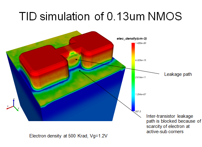
Total Ionizing Dose (TID) effect is one of the prominent effects on irradiated semiconductor devices. When a semiconductor device is exposed to ionizing radiation for a certain amount of time (thus there is a cumulative ionizing dose inside the device), leakage currents of the transistors may increase, threshold voltages and sub-threshold slopes may change. When the dose is high enough, the device might fail to work.
Simulation Approaches
What simulation can do in this field depends on how much details one understands about the physical (and electro-chemical) processes happening inside the device when it’s being irradiated. It also depends on how well one converts the understandings into equations and parameters, and how well the equations were coded. Parameter calibration is critical to the accuracy of simulation, and numerical method is critical to the speed.

Figure above gives the present situation of computer simulation in the field of TID. There are three steps:
- From radiation to dose distribution, it’s the problem of energetic particle transport. Modern Monte Carlo particle simulation can do the job precisely.
- From dose distribution to trapped charge distribution, it’s the problem of describing the behavior of electron, hole, H+ ion and H2 molecular (and maybe some other mobile species) inside insulators and its interfaces with semiconductors, including generation, drift, diffusion, trap-detrap, etc., usually in a very long period of time (days, months, even years). It’s a complicated process, not easy to simulate.
- From trapped charge distribution to leakage current increase, it’s the problem of charge carriers drift and diffusion in semiconductors under certain electric fields. Modern TCAD device simulation can do the job precisely.
There are a lot of efforts have been tried, and some are still being tried, on the 2nd step above.
Cogenda’s Work
Mechanism Simulation
Recently two comprehensive models on the TID effects were proposed, by N.L. Rowsey (2012) and I.S. Esqueda (2011), respectively. In each case, a set of equations were constructed to describe the transport of mobile species and reactions which leads to generation of oxide charge and interface states in devices subject to ionizing dose. When used with carefully calibrated parameters, both models have shown good agreement with experimental data.
Cogenda implemented both models in the Genius device simulator, and the Esqueda 2011 model has been included in the latest public release of the simulator.

The three figures below illustrate the simulated electron concentration of a 65nm NMOS transistor after receiving a total dose of (from left to right) 100, 300, and 500kRad. Color red represents more electrons, and blue means less. It can be seen that while ionizing dose increases, electron concentration gradually changes. That’s because the trapped charge in SiO2, especially in STI, increased.
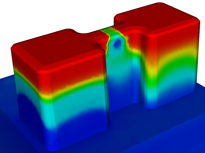
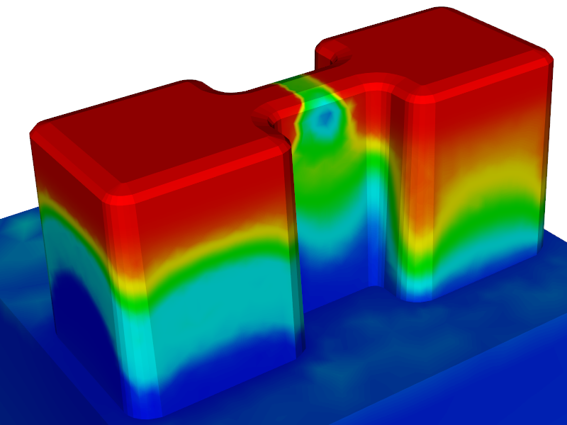
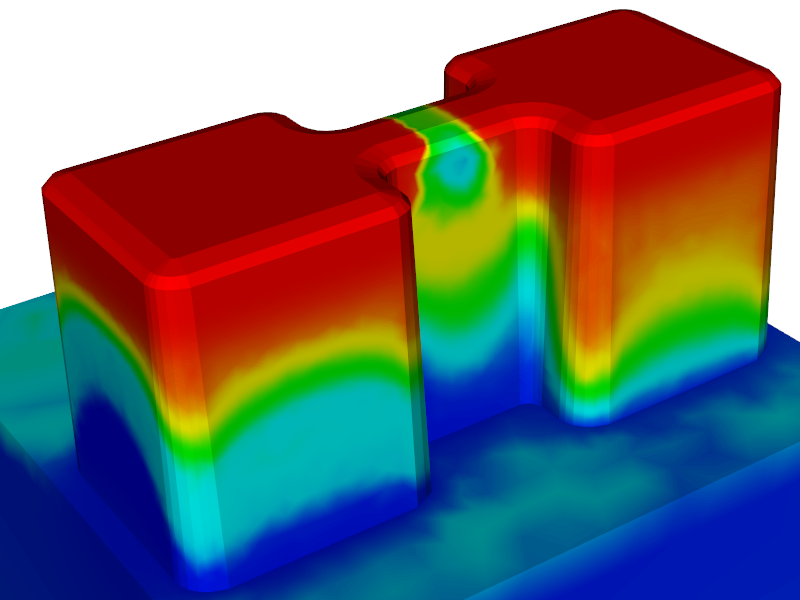
Simulated Result: electron concentration of a 65nm NMOS transistor with a total dose of 100, 300, and 500kRad
Thus for this transistor, leakage current increase is expected. It’s shown in figure below:
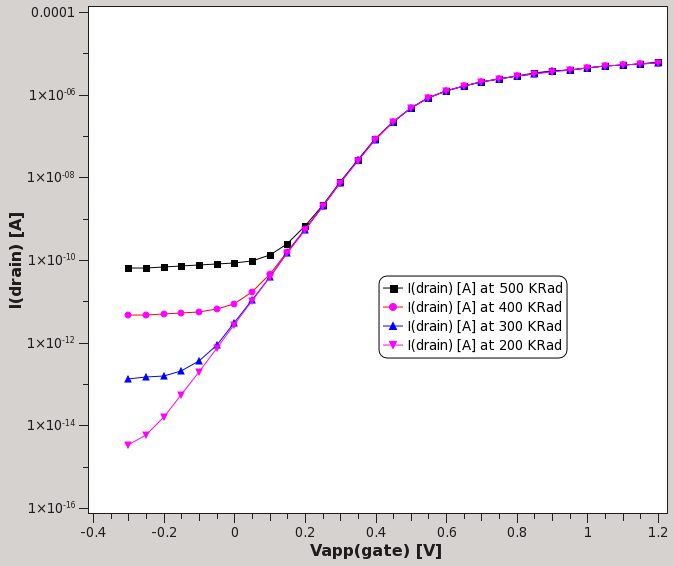
Simulated Result: Id-Vg curves at different levels of total dose
Such simulations can help us understand what’s really happening to irradiated semiconductor devices.
SPICE Model for TID Effect
To characterize TID effects in SPICE model, one convenient way is to use parasitic transistors. Figure below is a 130nm NMOS transistor with a dose of 500kRad. Two parasitic transistors are illustrated along with the intrinsic transistor.
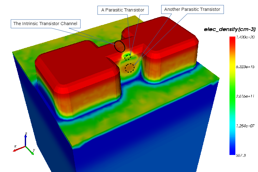
Cogenda provides SPICE model related services.
Hardening by Design
Such detailed simulations can help your hardening design in several ways:
- You can have detailed understandings of what happened to your chip when it is exposed to radiation.
- Thus you can figure out fancier designs for hardening.
- To test a hardening design, rather than manufacturing the chip and carrying out radiation experiments, using computer simulations can save you tons of money.
- To optimize confirmed designs, or to adapt them to new processes, you can also employ computer simulations.
Cogenda provides hardening design services.
On-Orbit Dose Prediction
Cogenda provides a software product CRad to predict TID and other effects on space orbits.
Ref.
- N. L. Rowsey, Quantitative modeling of total ionizing dose reliability effects in device silicon dioxide layers. 2012.
- I. S. Esqueda, Modeling of total ionizing dose effects in advanced complementary metal-oxide-semiconductor technologies. PhD thesis, Arizona State University, 2011.
