Next NANO
nextnanomat, nextnano++, nextnano³, nextnano.NEGF, nextnano.MSB
Powerful tools for the simulation of nanostructures and optoelectronic semiconductor nano devices.
Applications include nano transistors, LEDs, laser diodes, quantum dots, nanowires, quantum cascade lasers, HEMTs, photo detectors and solar cells.
PRODUCTS
We essentially offer five software tools.
- nextnanomat
Front End & Workflow Manager
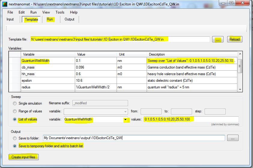
nextnanomat provides the graphical user interface (GUI) for the nextnano++, nextnano³, nextnano.NEGF and nextnano.MSB software. - nextnano++
Our Schrödinger-Poisson-Current solver written in C++. - nextnano³
Our Schrödinger-Poisson-Current solver written in Fortran. - nextnano.NEGF
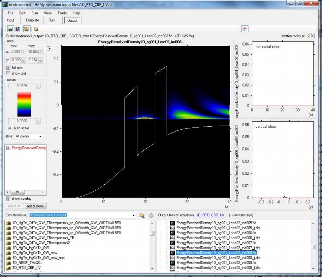
Our NEGF code for quantum transport in e.g. quantum cascade lasers (QCLs) and resonant tunneling diodes (RTDs) based on the nonequilibrium Green’s function method (NEGF). - nextnano.MSB
Our NEGF code for quantum transport in e.g. quantum cascade lasers (QCLs) and resonant tunneling diodes (RTDs) based on the multi-scattering Büttiker probe model (MSB).Whether you want to use nextnano++ or nextnano³ is up to you. Choose your flavor!


FEATURES
next generation 3D nano device simulator
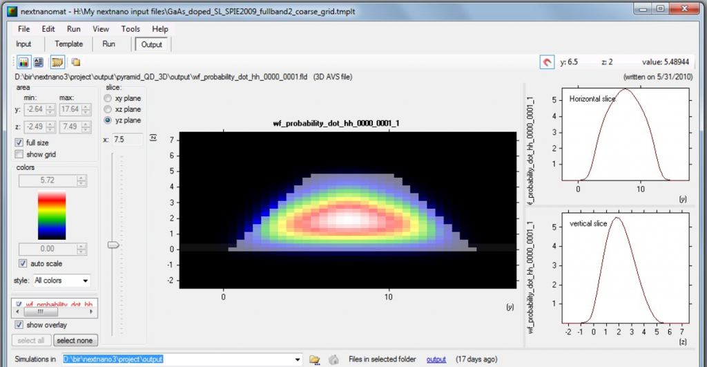
The nextnano++ and nextnano³ software are simulators for calculating, in a consistent manner, the realistic electronic structure of three-dimensional heterostructure quantum devices under bias and its current density close to equilibrium. The electronic structure is calculated fully quantum mechanically, whereas the current is determined by employing a semiclassical concept of local Fermi levels that are calculated self-consistently.
Simulating quantum dots, quantum wires, RTDs, MOSFETs, HEMTs, etc.
- includes group IV materials (Si, Ge, SiGe), all III-V and II-VI materials and its ternaries as well as lattice-matched quaternaries; the nitrides and the II-VI materials are available in the zincblende and wurtzite crystal structure
- flexible structures and geometries (1D, 2D and 3D)
- fully quantum mechanically, based on the 8-band k.p model within a finite differences grid
- includes strain, piezo and pyroelectric charges
- growth directions along [001], [011], [111], [211], … in short along any crystallographic direction
- equilibrium and nonequilibrium, calculation of current close to equilibrium (semi-classical), ballistic transport
- magnetic field
- optical absorption
- BIO-nextnano³
Semiconductors connected to an electrolyte solution (Poisson-Boltzmann equation)
