GTS Nano Device Simulator
Profound Physical Device Simulation @ N14, N10, N7, N5, N3
GTS Nano-Device Simulator (NDS) is the first complete and fully integrated solution for true physical simulation of nano-devices at the 10/14nm and 7/5/3nm nodes, including profound predictive simulation for new materials and architectures.
Your all-in-one Tool for Designing Emerging Devices
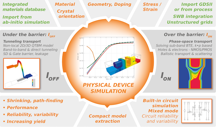
NDS includes models for all physical phenomena relevant for operation, performance, and reliability of nano devices, such as ballistic effects, scattering, direct tunneling, band-to-band tunneling, etc. In one single simulator setup, NDS can predict transistor performance parameters like electron mobility, ION, IOFF, sub-threshold slope, DIBL, leakage, and more — all based on physical simulation relying on material properties, and at short execution times that are well apt for daily use.
This makes NDS the only solid base for valid and sound predictions of device characteristics when using novel materials and new device designs and architectures.
Combined Approach to Get the Complete Picture
GTS Nano-Device Simulator uniquely integrates all models to cover IONas well as IOFF in one simulation setup:
Drive Current — NDS Phase-Space Transport (PST)
- Boltzmann transport equation
- Ballistic and dissipative transport
- Velocity overshoot
- Quantum resistance
- Performance enhancement by channel strain
- Important for on-current ION
Off-state Leakage — NDS Tunneling Transport (TT)
- Quantum-machanical transport
- Direct SD-Leakage
- Band-to-Band Source-Drain leakage
- Important for off-current IOFF
High-Mobility Channel Materials:
SSi, SiGe, Ge, InGaAs, … You Name It!
The integrated materials database includes properties for selected novel materials, such as strained Silicon, Silicon-Germanium, Germanium, or Indium-Gallium-Arsenide. The database is fully customer-editable, so you can easily add particular materials.
Material Properties from Ab-Inito Simulation
To populate the database, material properties can be imported from ab-inito simulation on atom level (see our joint event with Materialsdesign, Inc. at IEDM 2015), to fully integrate properties unique to each material – this way, profound predictions of device properties can be made even for less well-known or future materials.
Targeted Technology Nodes
Since GTS Nano-Device Simulator mostly operates with material-dependent constants rather than application-specific fitting parameters, it is not bound to a specific technology like conventional tools and models. Only the use of physical material constants allows to port simulation setups from one node to the next (device shrinking), or predicting device characteristics for a future node (path-finding TCAD).
Models and setups of GTS Nano-Device Simulator are highly portable, making NDS extremely versatile and efficient in daily use. Specifically, NDS targets the following technology nodes:
- 14/10nm FinFET, UTB FD-SOI
- 7/5nm Nanowire
What Makes GTS Nano-Device Simulator Unique?
GTS Nano-Device Simulator is the first available TCAD suite to combine all of the following features:
Phase-Space Transport (PST)
Over the barrier – see Fig.1–5.
- k·p-based
- Electron and hole transport for NMOS and PMOS
- Mass enhancement/degradation including confinement
- Strain effects/piezoresistivity “for free”
- “Direct” Pauli-exclusion
- Scattering
- Surface roughness
- Impurities
- Acoustic phonons
- Polar optical phonons
- Non-polar optical phonons
- Fast
- Adaptive in k
- Adaptive in energy
- Adaptive in r
- Powerful, proprietary algorithms & data structures
- Modular & flexible
- Problem separation in band structure, transport, and scattering
- Each part allows for customization
- Development kit (SDK) provided – more
Tunneling Transport
Under the barrier – see Fig. 6–10.
- Tunneling
- Direct tunneling
- Band-to-Band tunneling
- Real-space 2D/3D QTBM
- Confinement – guided current effect
- Ground-state energy – reduction of band-to-band window
- Accurate depiction of non-locality
- Fast
- Adaptive in energy
- Only transport under the barrier is calculated
- Powerful, proprietary algorithms & data structures
- Current-to-rate conversion
- No interference with other physical models, e.g. PST
- Isolate effects of direct Source/Drain tunneling and band-to-band (BTB) tunneling
- On-current consistent with semi-classical simulation
Reliability and Variability Simulation
Time-Zero Variability
- RDD: Random Discrete Dopands
- MGR: Metal Grain Roughness
- LER: Line-Edge Roughness
For more, see hot topic Device Variability.
Time-Dependent Variability
- BTI: Bias-Temperature Instability
- HCD: Hot-Carrier Degradation
For more, see hot topic Reliability/BTI.
- Fig.1: Si 8nm PMOS, ballistic distribution function in phase space
Application Example: Gate-All-Around FinFET
Demonatrating the usage of GTS Nano Device Simulator to model nMOS gate-all-around FinFET transistors: We show Id,lin, Id,sat, extraction of MOS parameters; effects of varying gate length, channel orientation, mechanical stress.
SeeGate-All-Around FinFET in our example gallery.
Tutorial: 20nm Nanowire Transistor
Take a step-by-step introduction to see how easy and efficient it is with GTS NDS to simulate a nanowire transistor and see the effects of chanel orientation and mechanical stress.
See Non-Planar Transistor Simulation from our tutorials.


